Semiconductors are one of the most fascinating areas of electronics manufacturing. The ability to “grow” almost irreducibly small integrated circuit components on silicon wafers has made an incredible amount of micronization possible. The theory has always been that as the chips got smaller, their processing power and speed would increase. This has been true for the past half a century, and even though this axiom is going through some interesting growing pains, its longevity is due, in part, to the process of photolithography.
The manufacture of semiconductors requires the utmost precision when creating the intricate patterns found on the inside of integrated circuits (IC) etched into the silicon wafers. The entirety of the semiconductor manufacturing process is extensive, deeply complex and has necessitated the creation of several specialty fields for highly skilled technicians to hone in on very particular aspects of the process.
The procedure begins with the formulation of a silicon ingot that gets sliced into extremely thin, highly-polished wafers about 1/40th of an inch thick and usually 6-12” in diameter. The wafers are prepared for photolithography through a series of polishing, chemical etching, heating, and rinsing steps. These are used to clean the silicon of particulate, moisture, and organic impurities that could get in the way of the wafer bonding with the photoresist, which is vital to the photolithographic process.
Getting the resist to adhere properly is a crucial aspect of the semiconductor manufacturing process. All subsequent processing, such as wet chemical etching, dry etching, and electroplating, rely heavily on the resist not peeling up from the wafer. If there is resist peeling at any point, the damage can be extremely costly.
Even though the microscopic transistors being built cost fractions of a cent to produce, the raw materials and, to an even greater extent, processing equipment is extraordinarily expensive.
A finished microchip can cost consumers hundreds or thousands of dollars, but if a wafer that is needed to build dozens or hundreds of these chips has an issue with one of its foundational layers - that’s a considerable amount of money down the drain.
Controlling this earlier stage in the life of the semiconductor involves ensuring that the wafer is clean and free of even the slightest chemical contamination. Through rinsing and surface manipulation techniques, such as the ones that were mentioned above, as well as the use of adhesion promoters, the bondability of the wafer surface is bolstered and can be reliably repeated with the right process controls.
Adhesion as a Critical Component of Photolithography
Creating the intricate features on the wafers typically requires the use of a multi-step process called photolithography, a printing method where UV light is employed to transfer patterns onto a photosensitive surface. However, silicon itself is not photosensitive, so a material called photoresist is applied to the surface of the silicon. The application of a photoresist film requires a strong bond between the photosensitive coating and the silicon substrate.
There are many ways for the adhesion of the resist to be disrupted by contaminants being introduced or not sufficiently removed during preceding steps.
For instance, during the slicing phase, particulate caused by the diamond saw cutting into the silicon ingot to the proper thickness. As the wafer is polished and cleaned using substances like acetone, isopropanol, DI water, and other cleaning and etching agents, the rinses may not be administered properly, or the DI water may not be as pure as hoped.
To learn more about how to use contact angle measurements as a powerful process control method, download our eBook: Predictable Adhesion in Manufacturing Through Process Verification
The surface must also be as free as possible from moisture, so a baking out thermal cleaning is often used to neutralize many contaminants and oxides. When the surfaces of the wafers are fairly hydrophilic (water-loving) and therefore can oxidize relatively easily. The resist requires that the wafer have a more hydrophobic (water-repellant) surface in order to adhere properly. The baking out process breaks the oxygen-hydrogen (OH) bonds on the surface of the oxidized wafer, which increases the hydrophobic character of the surface.
Using an Adhesion Promoter in Semiconductor Manufacturing
The purpose of cleaning the wafer is to get the surface to its most pure state, essentially where the molecules on the surface are only those that belong to the wafer material and none that have been added during the production or handling process.
An adhesion promoter does the exact opposite, in that its purpose is to offer a different, more attractive surface to the resist for bonding.
Silicon dioxide (SiO2) or sand, which the wafer is typically constructed of in the form of quartz, glass, or silicon, has native oxides that form polar OH bonds when exposed to atmospheric humidity because of this inherent hydrophilicity. This characteristic means it exhibits a poor affinity for the non-polar or low-polar molecules of the photoresist.
In order to make the wafer surface hydrophobic (water-repellent and thus photoresist-attractive),
non-polar molecules of adhesion promoters such as Hexamethyldisilazane (HMDS) or organic titanium compounds can be chemically bound on it.
How to Use HMDS to Get Great Photoresist Adhesion
When silicon wafers are first manufactured, water gas particles can be trapped within the silicon, thus causing imperfections in the single silicon crystal. These imperfections can lead to unwanted electrical characteristics in the finished device, costing manufacturers valuable time and money. HMDS creates a hydrophobic coating that repels the water molecules from the surface, aiding in reducing the risk of failure down the line. While the hydrophobic coating works well to repel unwanted water molecules, it also serves another purpose in helping manufacturers in the process.
HMDS is a primer agent used in coating semiconductors prior to the adhesion of a photoresist agent. HMDS forms a strong bond with the OH molecules on the surface of the silicon, and the methyl groups it leaves on the surface once it’s been deposited, aid in creating strong adhesion with the photoresist. The HMDS is a crucial component in semiconductor manufacturing; it creates a bridge of organic to inorganic molecules between the surface of the silicon wafer and the photoresist. Without it, the photoresist does not form a secure bond with the wafer.
The all-important HMDS has been used since before the 1970s. The dual purpose of the HMDS means it is absolutely critical to achieving good adhesion to ensure the photolithography etches a perfect pattern. The process of applying HMDS has been innovated on numerous times since the 1970s, and it has become one of the most impactful process improvements to the semiconductor industry, allowing manufacturers to ensure quality products.
The process was initially developed in the 1970s to ensure the dehydration process the silicon wafers undertook prior to HMDS coating was sufficient. When it was discovered that the wafers were scarcely ever dehydrated enough, a new process had to be developed. In the mid-1970s, semiconductor experts developed a process that baked the wafers in a large pressurized oven, in which the wafers underwent a series of vacuums and floods of heated gas to purge the chamber and the silicon wafers of any water molecules. If the water molecules are not sufficiently purged from the wafers, the HMDS will bond with the water molecules rather than the silicon, and the water molecules will evaporate, taking the all-important HMDS with it.
This process was perfected by Bill Moffat, founder of Yield Engineering Systems and a pioneering engineer in the front-end processing of semiconductors. Bill and his team concluded, after a series of experiments with vapor priming systems and HMDS deposition, that a 30-minute cycle of pressurizing and nitrogen exposure, along with the final HMDS introduction, was ideal for creating a surface that the photoresist would adhere to without failure.
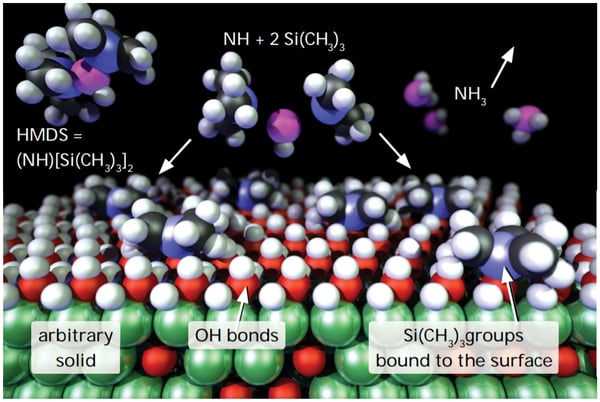
In this image, courtesy of MicroChemicals, a simplified version of the process is shown with HMDS fragmenting into Si(CH3)3 groups that cover the surface and release ammonia (NH3). The polar methyl groups create the kind of hydrophobicity necessary for resist adhesion.
The deposition process of the HMDS can be done with a couple of different techniques. A common way is to use a spin-coating method in a very similar fashion to how the resist is deposited. This method is not advised because vapor from the thick layer of HMDS deposits can cause issues for subsequent coating applications and just doesn’t offer reliable adhesion of the resist.

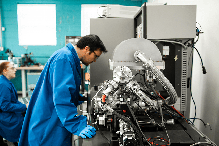
An alternative method is to use a vacuum deposition system such as the YES TA Series vacuum cure/vapor prime systems: 58TA and 310TA. The vacuum pulls in the proper amount of HMDS. On the side of the YES unit (as seen below) is a large test tube over a pint volume filled with HMDS. The YES final vacuum pull is to 1 Torr. Then a valve to the HMDS is opened, and a controlled, specific quantity of clean HMDS vapor is pulled into the chamber. HMDS vapor pressure at room temperature is 14 Torr, so you get 14 Torr of HMDS in the chamber. This allows for a uniform and necessarily thin film of HMDS on the surface.
How to Verify Wafer Surface Pretreatment and Predict HMDS Coating Effectiveness
HMDS effectively creates a hydrophobic surface on the wafer that increases the wettability (attraction) of the resist. However, the process is only as good as the wafer surface created through cleaning and treatment. Verifying the chemical compatibility of the wafer surface and the presence of a uniform coating of the HMDS helps assure manufacturers that the critical photoresist will adhere to the primed silicon.
Contact angle measurements are a relatively common way of testing the surface quality of the polished wafer and verifying the presence of the HMDS coating. The traditional method of conducting these tests takes place in a research lab using a stationary goniometer, which, while effective and useful for gathering crucial data, adds even more time and cost to an already expensive and time-intensive process.
Bill Moffat explains the criticality of process control for perfect adhesion this way, "The photolithography engineer faces requests to downsize constantly. If the circuit is 10% smaller, you get more circuits on the wafer and higher profits or cheaper circuits. This means an increasing need to control adhesion.
“If you have a small loss of control because of a ragged resist line,” Moffat says, “it does not matter until the critical dimensions you are creating approach the same size. A 1-mill transistor does not care about a submicron variation. A submicron transistor can be destroyed by it. As we look for submicron, we should be looking for control of resist adhesion using control of contact angle."
With recent advances in handheld and automated contact angle measurement systems, these tests can be conducted quicker and more efficiently than previously possible to achieve the micron-level amount of control Moffat explained was needed.
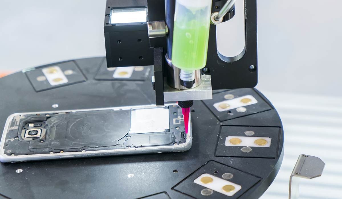
The technique works by depositing a drop of liquid, usually highly purified water, on the surface of the wafer and measuring to what extent that droplet wets out on the surface. This can indicate that it is ready to adhere to the HMDS coating and, once the coating is applied, can give quantitative evidence that the coated surface is suitably hydrophobic for the photoresist to bond well to.
When liquid molecules come in contact with the HMDS coating, the droplets are repelled, and thus they constrict into a spherical shape, causing a very large contact angle. The resist film is highly attracted to the hydrophobicity of the HMDS, making contact angle measurements a secure way of predicting the functionality of HMDS as an adhesion promoter.
The hydrophobicity of the HMDS-coated wafer typically depends on and is proportional to the amount of time the wafer was subjected to the HMDS vapor. And because HMDS is extremely hydrophobic, the amount of coating on the surface is readily detectable using a water contact angle. So much so that many of the most prominent semiconductor manufacturers today have contact angle requirements to validate the proper amount of HMDS on a wafer.
During Bill Moffat’s experimentation, he found that on a typical silicon wafer, the 30-minute cycle he devised created a surface with a 75° contact angle, which means the surface is hydrophobic enough to be highly attractive to the photoresist.
The HMDS coating ensures that the silicon bonds securely to the photoresist to allow for accurate photolithography. Precise lithography is crucial for the manufacture of integrated circuits for our growing digital world. Taking fast, accurate, and reliable measurements is the perfect way to reduce costly waste from the manufacturing process.
To learn how to use contact angle measurements as a powerful process control method, download our eBook on process validation techniques: Predictable Adhesion in Manufacturing Through Process Verification