Defining “clean” is actually more complicated than it sounds. Cleanliness can be in the eye of the beholder (I mean, we all had a college roommate who swore they were tidy, but let’s be honest…), and it can also be calculated and precisely managed to the nth degree. In regard to PCB cleanliness for electronics manufacturing, there has been one prevailing notion that has dominated the conversation for decades.
Ionic contamination has been a cleanliness concern for electronic assembly manufacturers for years. Ionic contamination can certainly lead to shorts in the circuitry of PCBs, but the problem is - the testing methods for this type of contamination are limited. They are not able to pinpoint areas of contamination, and they are not able to account for any forms of contamination beyond ionic forms, leaving out all organic residues.
Cleanliness is crucial for the predictable functionality of electronics because it:
- allows for confidence that conformal coatings will stick
- ensures no nefarious species are trapped underneath the coating
- increases reliability by removing threats of failure (like dendritic growths that cause shorts)
A Brief History of Electronics Cleaning
In the 1970s and 1980s, military and manufacturing standardization bodies like IPC wrote specifications for the cleanliness of electronic assemblies. These primarily looked at the removal of flux residue, which is the leftover residue from a protective layer put on circuit boards to support soldering and reflow processes by reducing oxidation. The standards also clarified acceptable levels of ionic cleanliness.
Download our checklist to diagnose the root cause of adhesion failures you’re experiencing in your PCB manufacturing process: Checklist: Adhesion Failure Root-Cause Analysis for Manufacturers
Flux residue needs to be removed because it can trap moisture and contaminants detrimental to adhesion, and it can short out closely spaced conductors on a circuit board (which became a much bigger issue as electronics shrank in size and the components became more compact on the boards).
The advent of no-clean flux seemed to solve many cleanliness issues and streamline manufacturing processes. But failures in coatings and shorts still remained to an extent that is unacceptable in high-reliability applications. As electronics found their way into hi-rel applications like medical devices, mission-critical systems for military and aerospace vehicles and aircraft, and automotive sensor systems, the need to remove flux residue and ensure complete dependability became a greater concern. Cleaning remained as important as ever.
So, now we are in a new era of cleaning electronic assemblies where it is crucial to clean and measure the totality of contaminants on a board.
How to Clean Printed Circuit Boards for High Reliability
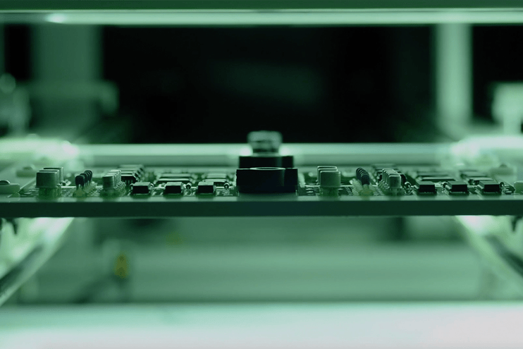
There are many options available for removing flux and cleaning away the majority of contamination found on boards that can cause inconsistent coatings or promote dendritic growth. The most common and effective cleaning method of choice is an aqueous bath and rinse cycle. Soluble contamination like ionic species, leftover flux residues, and basically all debris will be handled in industrial washes. Sometimes, although less frequently, manual cleaning is necessary to de-flux some residue that has plasticized in the curing ovens and becomes just too hard to remove with a bath alone.
Cleaning standards have not changed drastically over the years. When talking about ionic contamination, the IPC-TM-650 standard sets an acceptable range of 0.1 µg/in2 for military applications (0.65 µg/in2 for general applications) of sodium chloride (NaCl). But as reliability expectations have risen, this standard has had to be augmented. Merely cleaning for ionic contamination is not enough to prevent failures, and predominant cleaning methods are not meeting the challenge of high-reliability requirements.
As it becomes more and more clear that organic contamination needs to be cleaned and a chemically clean PCB surface is required for reliable coating adhesion, surface treatment processes using plasma have become increasingly common.
Plasma treatment systems are high-precision cleaning units that are able to target places on boards that are difficult to clean with traditional methods. Also, plasma is primarily used as a way of changing the chemical makeup of a board’s surface. By bombarding the surface with particular chemistry, molecular bonds are broken, and a highly active surface is created, making a very bondable situation. Through in-line automation, plasma is an excellent option for high-rate, high-reliability manufacturing.
Cleanliness Process Control to Create Predictable Outcomes
The debate about which cleaning standard and cleanliness testing method to adopt has ramped up recently as standards are expanding to include a more fulsome definition of cleanliness. Ion chromatography (IC), Resistivity Of Solvent Extract (ROSE) testing, Surface Insulation Resistance testing (SIR), and visual tests are all valuable tools to determine if an assembly is clean, and each carries both benefits and drawbacks.
While ROSE testing remains by far the most popular and accessible method of cleanliness testing, it is not without its faults. ROSE testers are popular because of their speed and relatively low price point, but they are not capable of detecting all forms of possible contamination, and the ionic contamination they do detect is averaged over the whole surface. So if the test detects any contamination at all, it cannot tell you where on the surface it is, and it assumes that all detected contamination is evenly spread across the board.
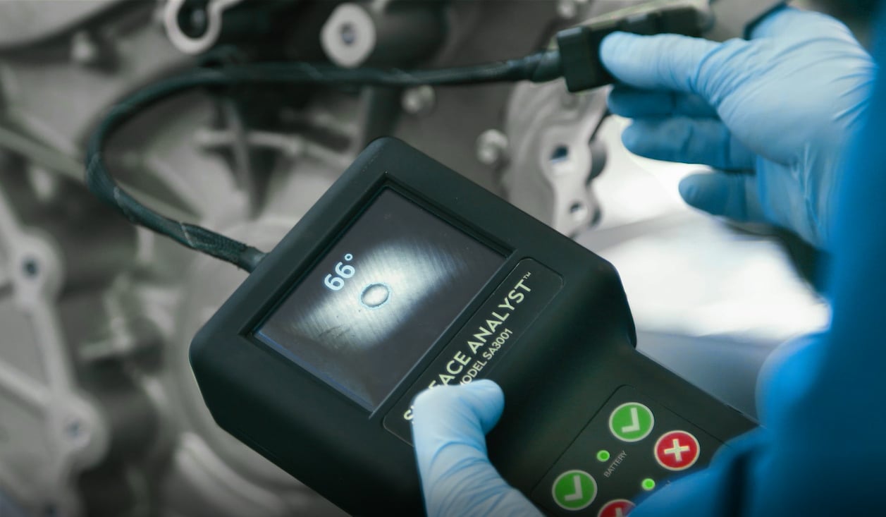
A very useful method of pinpointing contamination and getting a quantitative evaluation of organic contaminants is to use a water contact angle measurement. Water contact angle works by depositing a drop of water on the surface of a material and measuring to what extent the drop expands (wets out) or constricts (beads up). If the water is attracted to the surface because the chemical composition has a strong attractive force on the water, it will wet out. This correlates directly to how the conformal coating will respond to the surface. With this measurement in hand, you can effectively predict if your coating will bond well to your surface, and then it can be used to understand if your coating is uniform across the surface as well.
Water contact angle is an excellent process check for all cleaning methods. If you take a measurement before and after each cleaning and treatment step, these measurements can alert you to changes that you otherwise wouldn’t have been able to see. These measurements can be taken directly on the line with an automated device or used as a supply chain management tool at a quality checkpoint to inspect all incoming materials.
Some of the most dangerous assumptions made by electronics assemblers are:
- All bare boards coming from the fabricator are clean.
- All components going onto the board are delivered clean with no contamination issues
Right now, most manufacturers have to assume these things because there is no reliable way to check otherwise. Using a contact angle measurement to create a cleanliness specification when parts are received offers a way to track possible contamination introduction throughout the entire assembly and adhesion process. That way, you’ll be able to have real visibility into what is causing contamination and make all of your cleaning efforts as effective as possible.
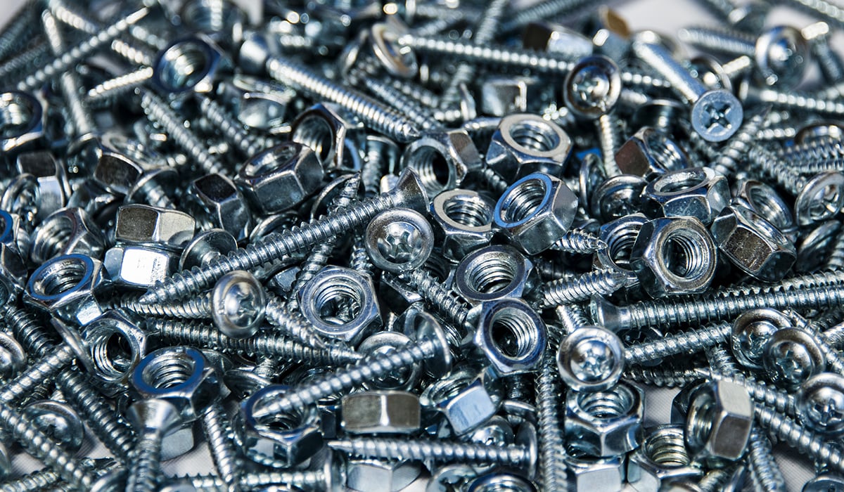
Looking at the image below, you can see there are a lot of bonding sites and potential places for adhesion failure on the surface of PCBs. All of these areas need to be fully cleaned and inspected so they are entirely prepared for bonding and coating.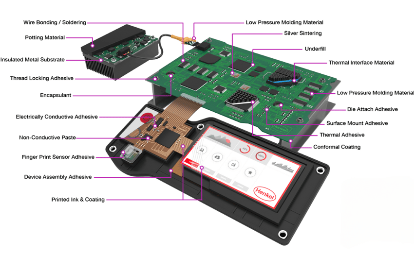
Redefine Clean
In order to control the totality of residues that cause coating failures and electrochemical migration (ECM) resulting in shorts, you need to have a definition of clean that includes all of the possible contaminants threatening your board.
Expectations of reliability are increasing, and cleaning methods need to rise to the occasion. The best way to ensure your cleaning is effective is to measure it. The most efficient way to measure cleanliness is to evaluate all of the materials involved at each step where contamination is possible and where cleaning occurs. These Critical Control Points need to be monitored through a data-driven test system that proves definitively that the surface is clean and bondable.
To learn more about diagnosing the root cause of adhesion failures in PCB manufacturing and how to control cleaning methods and supply chains, download our eBook: Checklist: Adhesion Failure Root-Cause Analysis for Manufacturers.